555 Circuits Part 1
A collection of 555 circuits using the 555 Timer as an astable oscillator with different duty cycles
We have seen in the last few tutorials that the 555 Timer can be configured with externally connected components as multivibrators, oscillators and timers, with timing intervals ranging from a few microseconds to many hours. As the 555 timer is one of our favourite, cheapest and easily configurable chips, let’s look at using it to create some different 555 circuits.
As we have seen previously, the 555 timer comes as a single device within an 8-pin dual-in-line package (DIP) or as the 556 device which has two 555 chips in a single 14-pin dual-in-line package. The two 555 timers within the 556 operate independently of each other but share a common VCC supply and ground (0V) connection.
The standard TTL 555 can operate from a supply voltage between 4.5 volts and 18 volts, with its output voltage approximately 2 volts lower than its supply voltage VCC. The 555 can source or sink a maximum output current of 200mA, (but it may get hot at this level), so the circuit variations are unlimited. Note that the CMOS versions of the 555, the 7555 and the 7556 may have different voltage and current ratings.
But first let us remind ourselves of some of the basic formulas we can use to calculate the oscillation frequency.
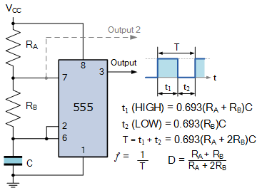
Where: t1 is the output high duration, t2 is the output low duration, T is the periodic time of the output waveform, ƒ is the frequency of the output waveform, and 0.693 = ln(2)
When connected as an astable oscillator, capacitor C charges through RA and RB but discharges only through RB.
Thus the duty cycle D is determined by the ratio of these two resistors. With the proper selection of resistors RA and RB, duty cycles of between 50 and 100% can be easily set.
The total time period T is given as the capacitor charging time, t1 (Output High) plus the discharging time, t2 (Output Low) as the capacitor charges and discharges between 1/3Vcc and 2/3Vcc respectively.
In this mode of operation the charging and discharging times and therefore the frequency, ƒ which is given as: 1/T, is independent of the supply voltage.
Simple 555 Oscillator
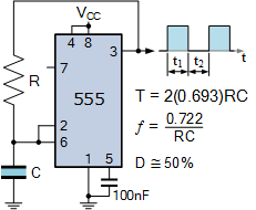
The basic 555 oscillator circuit is very versatile, and we can create a number of interesting variations from it. The simplest 555 free-running astable oscillator circuit connects pin 3 (output) directly to the timing capacitor via a single resistor as shown.
Simple 555 Oscillator

When the output at pin 3 is HIGH, the capacitor charges up through the resistor. When the voltage across the capacitor reaches 2/3Vcc, pin 6 causes the output at pin 3 to change state and goes LOW.
The capacitor now discharges back through the same resistor until pin 2 reaches 1/3Vcc causing the output to change state once again. The capacitor continually charges and discharges between 2/3Vcc and 1/3Vcc back and forth through the same resistor creating a HIGH and LOW state at the output, pin 3.
As the capacitor charges and discharges through the same resistor, the duty cycle of this basic arrangement is very close to 50% or 1:1. The series of square wave output pulses produced have a cycle time (T) equal to approximately 2(0.693)*RC or 2lin(2)*RC. The output waveform frequency (ƒ) is therefore equal to: 0.722/RC.
So for example, if we want to generate a 1kHz output square-wave waveform, then R = 3.3kΩ and C = 220nF using preferred component values.
Fastest 555 Oscillator
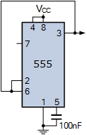
By varying the value of either R or C the 555 astable multivibrator circuit can be made to oscillate at any desired output frequency. But what is the maximum frequency of oscillations we can produce from a single 555 timer chip.
To get the 555 to operate at its highest frequency, it is necessary to continuously retrigger it the instant the output changes state, from high to low, or low to high. The fastest switching speed can be obtained by removing both the R and C timing components and feeding the output signal directly back the trigger inputs.
By connecting the output, pin 3 to both the trigger input, pin 2 and the threshold input, pin 6, every time the output changes state it re-triggers the 555 to change state again. However, the output waveform will not be symmetrical or a square wave but a series of negative pulses.
The highest oscillation frequency obtained using this arrangement will depend on the supply voltage, the type of 555 chip used, TTL or CMOS and the manufacturer as the internal circuitry differs from manufacturer to manufacturer. But it is possible to produce an output frequency as high as 350kHz at 5 volts.
Slowest 555 Oscillator
If we go back to the original 555 oscillator circuit and replace the timing capacitor with a large value electrolytic, such as a 220uF or a 470uF capacitor, by selecting the appropriate timing resistor the frequency of oscillation can be reduced to much less than 1Hz. If this is the case, then the 555 circuit stops becoming an oscillator and becomes a timer or delay circuit whose pulse width could be 10’s of seconds.
555 Timer Circuit
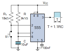
In this time delay circuit, the threshold, pin 6 and the discharge, pin 7 are tied together at the junction of the RC timing components and the output remains LOW and stable until the 555 is triggered into action by the application of a negative pulse on pin 2.
The trigger pin 2, is held HIGH via resistor R1 until the pushbutton switch, S1 is closed. Operation of S1 momentarily shorts pin 2 to ground and therefore below 1/3Vcc initiating the delay cycle.
Once tiggered the output on pin 3 switches HIGH for some pre-calculated duration determined by the circuits RC time constant and will not respond to any additional triggering of switch S1 until after the timed delay period has been reached, at which point the output at pin 3 returns LOW again.
This makes this manually triggered monostable circuit useful in switch debounce applications as a single pulse is created no matter how many times the switch is depressed. The width of the monostable output pulse period in which the output is HIGH is given as: 1.1RC in seconds, where R is in Ohms and C is in Farads.
So for our simple 555 time delay circuit, the output delay in which the output is in a HIGH state is calculated as: 1.1*9100*10*10-6 = 100ms. By selecting appropriate values of R and C output delays of a few micro-seconds to many hours can be obtained. However, for long timing delays requiring large value electrolytic capacitors, the timing period is generally not that accurate as an electrolytic capacitors tolerance can be extremely large, upto +/-50%.
This can be overcome by changing the timing resistor to a potentiometer to compensate for the capacitor’s tolerances, or by selecting low leakage electrolytic capacitors. In practice, the timing resistor should not exceed about 10MΩ or a timing capacitor greater than 470uF as both of these combined would give a delay pulse of about 5170 seconds or about 1.5 hours.
Modified Duty Cycle
We said previously that the duty cycle, that is the ratio of ON time to total cycle time, is limited to between 50% and 100% for the standard 555 oscillator circuit. But some applications may require a specific duty cycle to be set below 50%, that is the t1 (HIGH) time is less or shorter than the t2 (LOW) time which are set by the ratios of RA and RB.
As the resistance of RA becomes much larger than RB, the duty cycle increases towards unity (100%) as RB approaches zero.
Likewise, as the resistance of RB increases with respect to RA, the duty cycle approaches 50% (or 1:1) giving the output waveform a more square-wave appearance. However to get a full 50% duty cycle, RA would need to be zero Ohms which is not allowed as this would short out VCC to ground through the discharge pin 7.
One way of achieving a lower than 50% duty cycle is to include a diode within the RC timing circuit as shown.
50% Duty Cycle
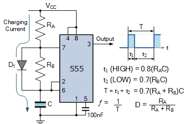
The addition of diode, D1 across pins 6 and 7 of the basic 555 oscillator circuit, shorts out resistor RB during the charging cycle.
The diode, which can be any general purpose silicon diode, allows the capacitor to charge directly from RA, as RA and D1 are effectively in series removing resistor RB from the charging cycle, although a very small leakage current will still flow through RB.
During the discharge cycle when the output at pin 3 is LOW, diode D1 is reverse biased so the circuit functions the same as before discharging through resistor RB and into pin 7 of the 555.
Thus during the charging cycle when the output is HIGH, RA and C control the t1 timing period, while during the discharging cycle when the output is LOW, RB and C control the t2 timing period.
Note that because of the presence of diode, D1 across RB, the diodes 0.7 volt forward voltage drop makes the circuit more sensitive to variations in supply voltage, Vcc. Thus the t1 timing expression is modified to approximately 0.8RC to account for this diode drop.
Improved Duty Cycle
We can improve on the previous circuit by adding a second diode, D2 in series with the discharging resistor, RB as shown.
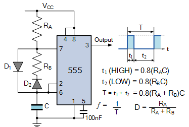
With the inclusion of D2, any parallel leakage current flowing through RB during the charging cycle is completely blocked as diode, D2 is reverse biased during this timing period.
During the discharging period, the capacitor discharges back through the series connection of D2 and RB as diode D1 is reverse biased during this cycle.
Thus both the charging and discharging paths for the timing capacitor become identical as the timing capacitor charges through RA and D1 and discharges through RB and D2 allowing for either timing period to be adjusted without affecting the other.
One interesting version of the improved duty cycle circuit using diodes, is that if you make the two timing resistors, RA and RB identical, that is RA = RB, the duty cycle will be exactly 50% producing a square wave output waveform.
Again the standard 555 astable oscillator equations are modified slightly to account for the inclusion of the diodes, and as before, due to the forward diode voltage drops, the timing periods are sensitive to supply voltage variations.
Fully Independent Timing Periods
We can improve once again on the above circuit by replacing the fixed value resistor, RB with one or two potentiometers is series with the two diodes. The inclusion of variable resistors would allow for fully independent variations in the RC charging and discharging timing periods as shown.
Fully Independent 555 Oscillator
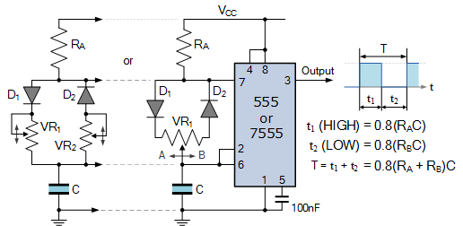
The timing circuit on the left shows the use of two potentiometers within the oscillator design. Using two potentiometers, VR1 and VR2, one each in series with the diodes.
The timing period for both the charging cycle (output high) and the discharging cycle (output low) can now be independently adjusted allowing full control over the duty cycle without affecting the output frequency. A simpler alternative variation on the previous circuit is by using a single potentiometer to control the two output timing periods at the same time as shown on the right hand circuit.
With the potentiometers wiper arm at its center position, the resistive value between point A and the wiper is equal to the resistive value between point B and the wiper. Thus the value of RB now becomes the value of VR1 and the duty cycle of the output waveform will be equal to 50%. Thereby producing a pulse modulated square wave shaped output waveform.
As the potentiometers wiper arm is varied from the center to point A, the duty cycle decreases. Likewise, as the potentiometers wiper arm is varied in the reverse direction from the center to point B, the duty cycle is increased. Thus the duty cycle of the output waveform can be varied from low to high, without any major changes to the output frequency.
We can take this idea one step further by converting a 50% duty cycle 555 astable circuit into one which allows us to vary tON to the tOFF times similar to the previous circuit. This ON/OFF (Mark/Space) ratio can be altered by adding a single diode and potentiometer (or one diode and two fixed resistors) as shown.
Varying the 555’s Duty Cycle
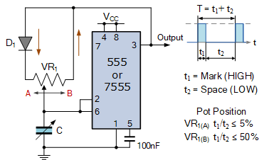
When power is first applied, the timing capacitor C1 is uncharged and output (pin 3) goes HIGH, so C1 quickly charges up via the forward-biased diode, D1 and one half of the potentiometer, VR1.
When pin 6 (Threshold) of the 555 detects 2/3 Vcc, output pin 3 switches LOW and capacitor C1 slowly discharges back through the other half of the potentiometer, as now the diode is reverse-biased, until pin 2 (Trigger) detects 1/3 Vcc causing the output, pin 3 to switch back HIGH again repeating the cycle once again.
The amount of time that the 555’s output is HIGH is called the “MARK”, and the amount of time when the 555’s output is LOW is called the “SPACE”. So by varying the potentiometer between point “A” (lowest) and point “B” (highest) we can alter the mark-to-space ratio (its Duty Cycle) of the output waveform between about 5% (position A) and a maximum of 50% (position B). Remember that if the Mark and Space lengths are the same then the output will be 1:1.
The advantage of this circuit is that we can produce short Mark (HIGH) lengths or pulses of time with very long lengths of Space (LOW) periods for all sorts of pulse and timing applications. If we reverse the direction of the diode, D1 we can create a timing circuit with a short Space but long Mark period, that is short OFF pulse but long ON duration.
The disadvantage of this basic variable duty cycle circuit is that the duration of the timing period changes as the potentiometer is adjusted due to the interaction of the two halves of the potentiometer. To compensate for this, if a fixed timing period T is required then the value of the timing capacitor, C1 must be adjusted or changed.
One very good use of either variable timing circuit is in controlling the speed of DC motors using pulse width modulation.
Pulse Width Modulation Motor Control
Pulse width modulation or PWM, is a way of controlling the average voltage value applied to a load by constantly switching it ON and OFF at different duty cycles. Rather than control the rotational speed of a motor by carefully applying less and less voltage to it, we can control its speed by alternatively switching the voltage fully ON and OFF in such a way that the average ON time produces the same effect as a varying the supply voltage.
In effect the control voltage applied across the terminals of the motor is controlled by the duty cycle of the 555’s output waveform which in turn controls the speed of rotation. We could also use this pulse width modulation method to control the brightness of a lamp or LED.
Pulse Width Modulation Control
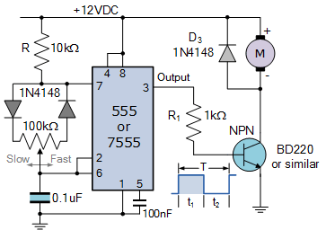
The speed of rotation of the DC motor is controlled using the potentiometer which inturn varies the duty cycle of the output waveform from about 5% to 95%. Resistor R1 limits current flow into the base of the switching transistor, and diode D3 is used in parallel with the motor to suppression and voltage transients as the motor is switched ON and OFF.
The switching transistor given in the example is a BD220 NPN Power transistor, rated at 70 volts, 4 amps, but any equivalent transistor would do provided it can safely handle the motor load current. The switching transistor may require a heatsink to dissipate the heat.

